By Tyrone Burke
Photos by CERN
The Large Hadron Collider is the largest machine on Earth – and one of most complex scientific instruments ever built. It uses powerful electromagnets to propel beams of charged particles at nearly the speed of light, and manipulates these beams into controlled collisions that create showers of billions of tiny particles. Most of these particles are not especially noteworthy, but there are some that can reveal the underlying physical properties of our universe.
Operated by the European Organization for Nuclear Research (CERN), the Large Hadron Collider consists of two 27-kilometre circular tubes buried deep underground along Switzerland’s border with France. Powerful compressors remove air from these tubes, and beams of particles are propelled in opposite directions through them. The tubes are lined with more than 1,200 large magnets that keep particles centered inside, so they do not collide with the machine itself.
Along the circuit, there are 16 radiofrequency cavities – metallic chambers that maximize resonance to create a powerful electromagnetic field. This field oscillates 400 million times each second, which separates the beams of particles into numerous bunches. As the particles pass each radiofrequency cavity, their electromagnetic force accelerates particles to ever greater speeds until they reach their maximum velocity — 99.999999 per cent of the speed of light.
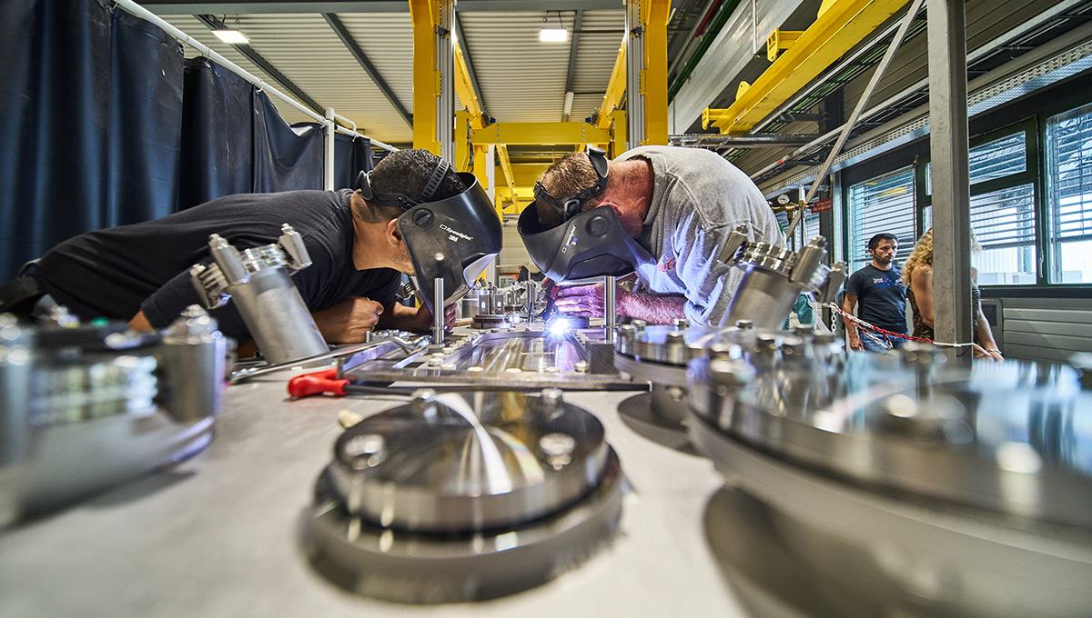
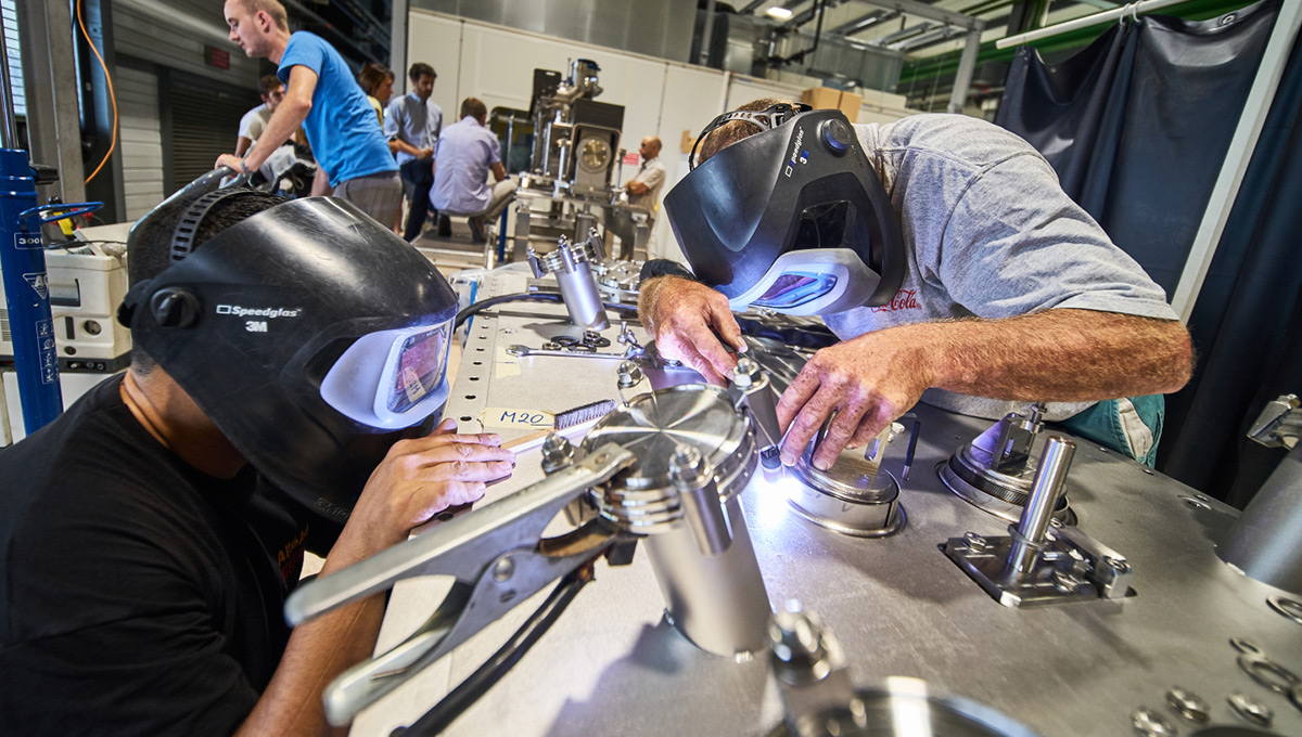
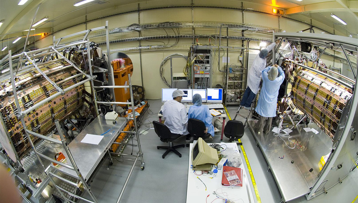
Welding and assembly of the HL_LHC superconducting crab cavities
Finally, another set of magnets focuses those bunches of particles, directing them to collide within one of CERN’s four major detectors. This results in a shower of particles, and a lot of radiation. The sensors in CERN’s detectors need to be sensitive enough to detect subatomic particles, and the chips that process that data must be capable of recording more than a billion particle interactions per second. And all of this needs to happen in an environment where radiation levels approach those at the core of a nuclear reactor.
Experimental physicists at Carleton are validating the new sensors and readout chips that will be used in the Inner Tracker of CERN’s largest detector: ATLAS. The Higgs boson was first observed in ATLAS in 2012, and the facility is being upgraded as part of the High-Luminosity Large Hadron Collider project. Slated for completion in 2027, the facility upgrade will significantly improve the Large Hadron Collider’s performance – and enable experiments that seek to demonstrate the existence of dark matter and other dimensions.
In particle accelerators, luminosity is a measure of how many particles can pass through a particular space in a set amount of time. More particles mean more collisions to observe and study. The new High Luminosity Large Hadron Collider will increase the accelerator’s luminosity by an order of magnitude – and similarly increase the number of particle collisions it can generate.
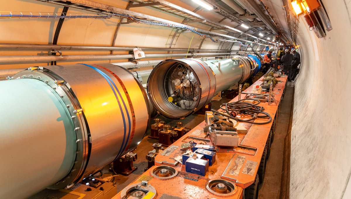
The High Luminosity upgrade gets underway with the installation of two HL-LHC Connection Cryostats
To accomplish all of this, significant hardware updates will be needed.
“We need to be able to detect individual elementary particles like a single electron,” says Thomas Koffas, an associate professor of Experimental Particle Physics at Carleton University.
“The new sensors are so sensitive that if you breathe on them, they will most likely be damaged.
“But in the Inner Tracker of ATLAS, they will be exposed to the full blast of the radiation. There is nothing in front of them, and there will be thousands of particles coming at each sensor during every collision. We want to be able to catch them all. To see what they are, and decide whether we care about a particular collision, or whether we drop it, and wait for the next one.”
The Inner Tracker has about 200 square metres of surface area, and about three-quarters of it will be covered with sensors that measure roughly 10 centimetres by 10 centimetres. This is extremely large for a sensor. Most are only a few millimeters across.
“Maintaining electrical performance over such a large surface area was one of the major challenges,” says Koffas.
“The sensors need to be able to hold at least half a kilovolt without breaking down. The larger the area of a semiconductor, the more difficult it is to achieve this.”
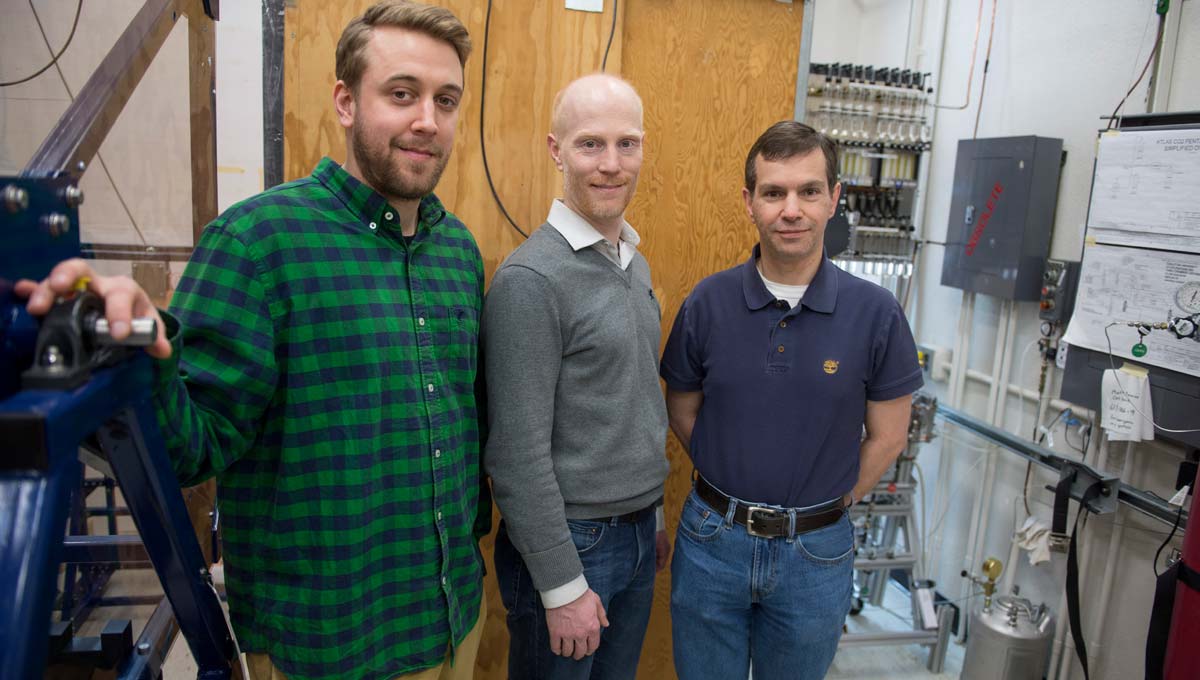
From left to right: Carleton master’s student, Robert Hunter, Prof. Dag Gillberg, and Prof. Thomas Koffas (Photo: Justin Tang)
The project’s R&D was led by CERN’s optoelectronics and microelectronics team. Carleton joined the initiative in 2014, and contributed to the stereo annulus geometry of the sensors’ silicon wafer design. Because of the irregular shape of the ATLAS Inner Tracker, eight different sensor shapes are needed. To correct for the irregularities, the researchers needed to incorporate rotation angles into the designs. Final prototypes were approved in 2019, and the first sensors were shipped this spring to Japan’s Hammamatsu Photonics.
Inside ATLAS, each sensor will transmit data to Application-specific integrated chips (ASIC) that record what they have detected. These chips were custom designed for this application by the CERN microelectronics department, in collaboration with Carleton and the Rutherford Appleton Labs in Oxford, U.K. The ASIC chips are being manufactured in Vermont by Global Foundries, and there will be more than 300,000 installed during the upgrade. Every one of them must be capable of processing about 640 megabytes of data in the brief moment in which a particle shower occurs. The stakes are high. If any sensor or chip fails during an experiment, data will be lost. This could preclude a major discovery.
To ensure that all chips and sensors meet the exacting performance standards, each sensor and chip will be tested individually. Carleton is the main beta tester for the ASIC chips, and will test about a quarter of the sensors. To meet the project’s demands, Carleton physicists are teaming up with the Department of Electronics and DA-Integrated, a local microelectronics testing company and the only firm so far that has demonstrated the ability to test the chips. DA-Integrated has been awarded a seed contract, and invited to participate in a tendering process — the first time that a Canadian company has been invited to do so.
To avoid damaging the sensors, testing needs to take place in purified air free of dust and moisture. The sensors’ electrical performance will be tested at a clean room in the Carleton University Microfabrication Facility in the Mackenzie Building, while mechanical performance and a visual inspection will take place at the FANSSI nanofabrication facility in the Minto Centre for Advanced Studies in Engineering.
A silicon tracker being worked on in the cleaning room ATLAS SR1
Chip testing will take place at the DA-Integrated facility in Stittsville, just outside Ottawa. There, each chip’s processing power will be validated using a suite of tests developed by experimental physicists at Carleton and Oxford University to test prototypes during the R&D process.
“There is a wafer with more than 400 chips on it, and a machine tests each chip in sequence. Over a few seconds, it runs several hundred tests to make sure it is fully operational,” says Dag Gillberg, an associate professor of Physics who is working on the project.
“If it fails any test, the chip is removed and won’t be sent to CERN.”
It’s critical that every component is up to the task.
“We only have one shot. Once we start, they will be in the detector for 12 years,” says Gillberg.
“We won’t be able to fix it after one year, if it is damaged. That’s why we have to be so careful. We need to make sure that everything is working exactly right.”